MBE-MoS2三角形单晶
货号:100891 编号:Mk1091
CAS号:1317-33-5 规格:1*1cm2;样品尺寸:5-25 μm
包装:原包装进口 保质期:
保存条件:
库存: 0 件
碳纳米笼
货号:100891 编号:Mk1091
CAS号:1317-33-5 规格:1*1cm2;样品尺寸:5-25 μm
包装:原包装进口 保质期:
保存条件:
请选择规格参数
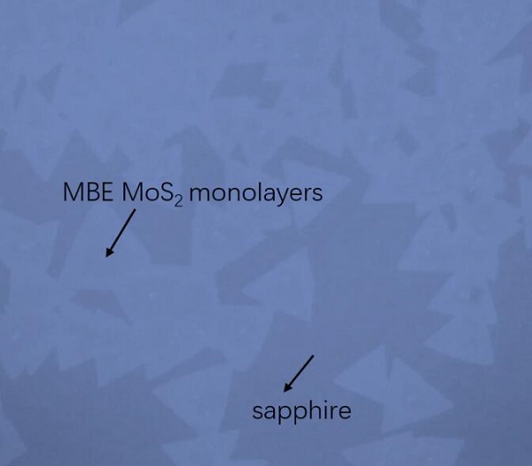
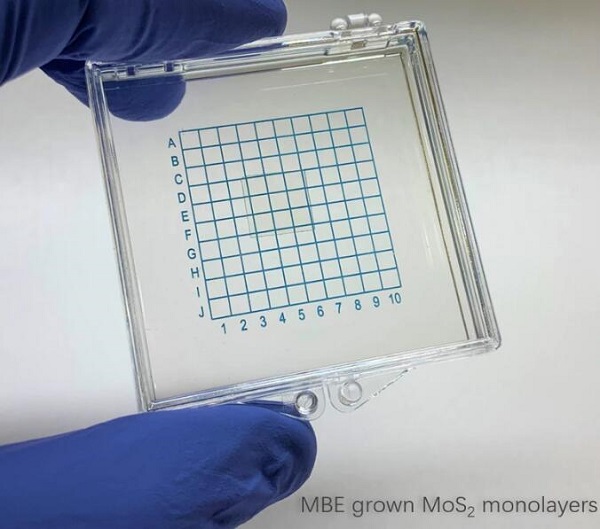
样品照片:

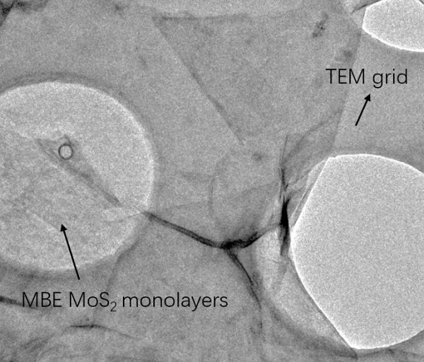
TEM:
MBE设备图片:

Raman:

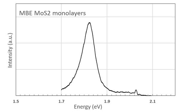
PL:
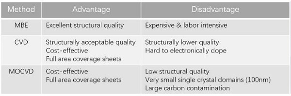
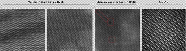
不同生长方法样品区别:
HRTEM:
Description:
World's first molecular beam epitaxy (MBE) grown MoS2 monolayers. MBE is an epitaxial method for single-crystal quality film deposition which offers high crystallinity and reduced defect density compared to chemical vapor deposition (CVD) or metal-organic chemical vapor deposition (MOCVD) techniques (see HRTEM images below). MBE growth of MoS2 monolayers take place in a MBE chamber at a base pressure of 8E-9 Torr and deposition rate is extremely slow (5-100 atoms per second) to reach structural perfection. Typical MBE growth produces monolayer thick MoS2 isolated triangles on double-side polished c-cut sapphire. Currently, MBE MoS2 is only offered on sapphire substrates but in the near future our MBE substrates will also include mica, graphite, and gold.
Sample Properties:
Sample size:1cm x 1cm square shaped
Substrate type:Double side polished c-cut sapphire
Coverage:Isolated triangles but may reach some continuity
Electrical properties:Direct gap excitonic semiconductor
Crystal structure:Hexagonal Phase
Unit cell parameters:a = b = 0.33 nm, c = 1.292 nm, α = β = 90°, γ = 120°
Production methodMolecular beam epitaxy (MBE)
Characterization methods:Raman, photoluminescence, TEM, XRD, and others

