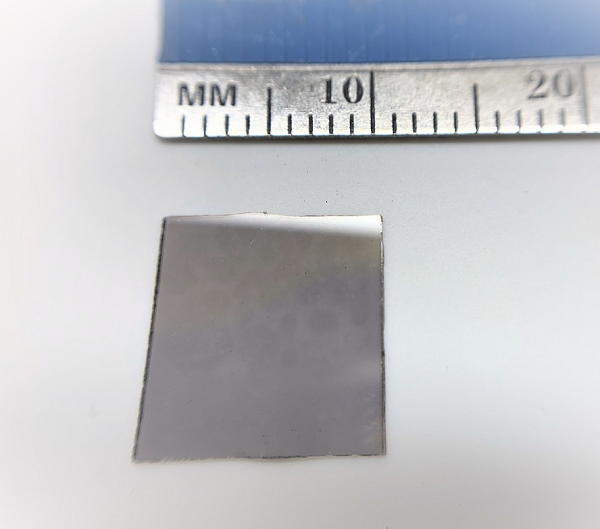
PdS2 is vdW material with excellent catalytic and semiconducting properties. Full area coverage PdS2 layers on c-cut sapphire substrates has been grown using modified chemical vapor deposition technique. Sample size measures 1cm in size and the entire sample surface contains PdS2 sheets. Synthesized full area coverage PdS2 is highly crystalline.
Sample Properties:

Specification.
- Identification. Full coverage 100% monolayer PdS2 uniformly covered across c-cut sapphire
- Physical dimensions. one centimeter in size. Larger sizes up to 2-inch wafer-scale available upon requests.
- Smoothness. Atomically smooth surface with roughness < 0.15 nm.
- Uniformity. Highly uniform surface morphology. PdS2 monolayers uniformly cover across the sample.
- Purity. 99.9995% purity as determined by nano-SIMS measurements
- Crystallinity. High crystalline quality, Raman response, and photoluminescence emission comparable to single crystalline monolayer flakes.
- Substrate. c-cut Sapphire but our research and development team can transfer PdS2 monolayers onto variety of substrates including PET, quartz, and SiO2/Si without significant compromisation of material quality.
- Defect profile. PdS2 monolayers do not contain intentional dopants or defects. However, our technical staff can produce defected PdS2 using a-bombardment technique.