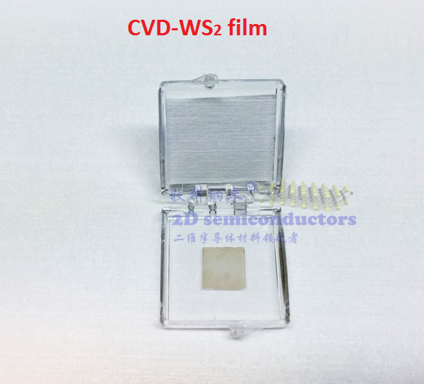
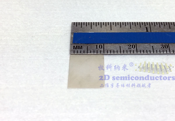
样品照片:

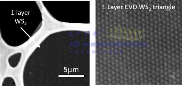
HRTEM:
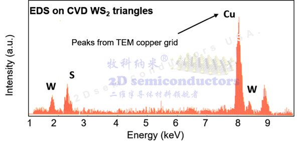
EDX:
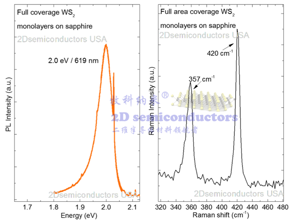
Raman和PL光谱:
Description:
Isolated monolayer thickness WS2 are grown onto c-cut (0001) sapphire substrates. This particular product contains monolayer thickness WS2 triangular flakes randomly distributed across sapphire substrate. While some regions reach continuity with coalesced WS2 triangles, this sample contains well-separated triangles for advanced spectroscopy, microscopy, and electronic measurements. Synthesized monolayer WS2 triangles are highly luminescent and Raman spectroscopy studies also confirm the monolayer thickness.
Growth method: Our company synthesizes these monolayers using chemical vapor deposition (CVD) using highest purity (6N) gases and precursors in semiconductor grade facilities to produce crystalline and large domain size samples (1-50um). This is unlike commonly used MOCVD process wherein defects are very very large and domain sizes are small (10nm-500nm). Our samples are always highly luminescent and highly crystallized
Sample Properties
| Sample size | 1cm x 1cm square shaped |
| Substrate type | (0001) c-cut sapphire |
| Coverage | Isolated and partially merged monolayer triangles |
| Electrical properties | 2.0 eV Direct Bandgap Semiconductor |
| Crystal structure | Hexagonal Phase |
| Unit cell parameters | a = b = 0.312 nm, c = 1.230 nm, α = β = 90, γ = 120° |
| Production method | Low pressure Chemical Vapor Deposition (LPCVD) |
| Characterization methods | Raman, photoluminescence, TEM, EDS |
Specification.

