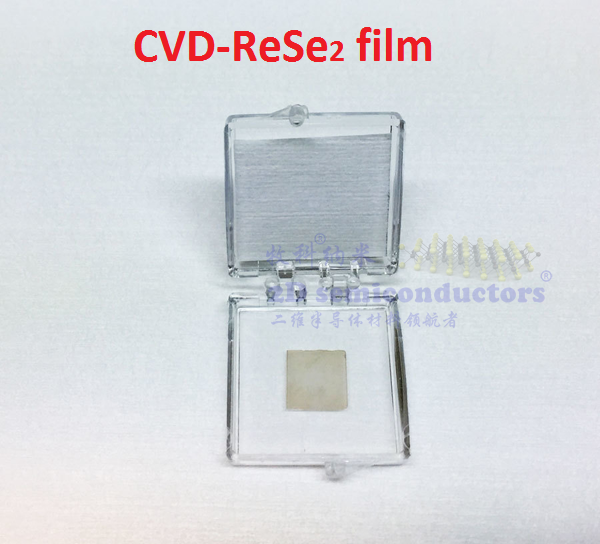
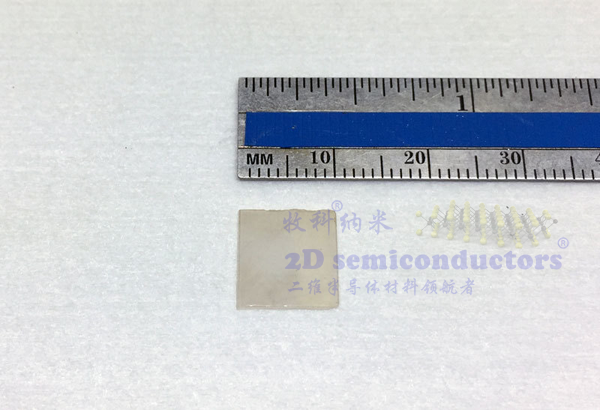
样品照片:

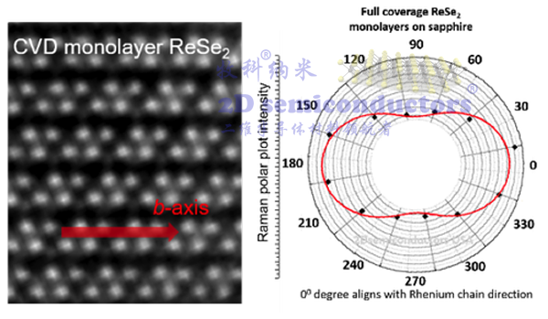
HRTEM:
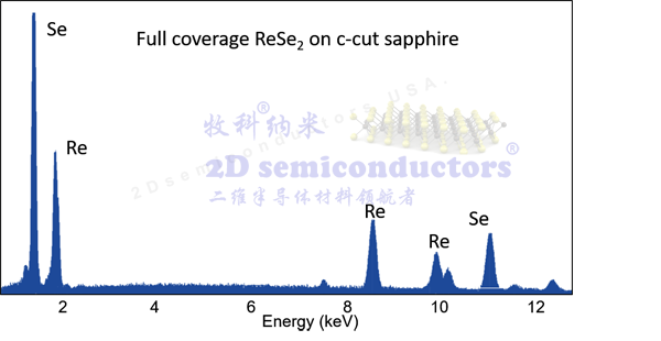
EDX:
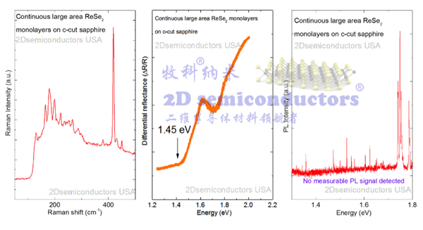
Raman和PL光谱:
Description:
This product contains full area coverage ReSe2 monolayers on c-cut sapphire substrates. Sample size measures 1cm in size and the entire sample surface contains monolayer thick ReSe2 sheet. Synthesized full area coverage monolayer ReSe2 is highly crystalline, some regions also display significant crystalline anisotropy.
Growth method: Our company synthesizes these monolayers using chemical vapor deposition (CVD) using highest purity (6N) gases and precursors in semiconductor grade facilities to produce crystalline and large domain size samples (1-50um). This is unlike commonly used MOCVD process wherein defects are very very large and domain sizes are small (10nm-500nm).
Sample Properties
| Sample size | 1cm x 1cm square shaped |
| Substrate type | Sapphire c-cut (0001) |
| Coverage | Full monolayer coverage |
| Electrical properties | 1.45 eV Anisotropic Semiconductor (Indirect Bandgap) |
| Crystal structure | Distorted Tetragonal Phase (1T’) |
| Unit cell parameters | a = 0.656 nm, b = 0.672 nm, c = 0.674 nm, α = 91.74°, β = 105°, γ = 119° |
| Production method | Atmospheric Pressure Chemical Vapor Deposition (APCVD) |
| Characterization methods | Raman, angle resolved Raman spectroscopy, photoluminescence, absorption spectroscopy TEM, EDS |
Specification.

