
库存: 0 件
碳纳米笼
货号:100876 编号:MK1076
CAS号: 规格:
包装:原包装进口 保质期:3个月+
保存条件:室温密封
请选择规格参数
| 样品名称 | 磷化锗GeP晶体 |
| 性质 | 半导体 |
| 带隙 | 待实验确定 |
| 参数 | 尺寸:~ several mm |
| 应用 | 半导体电子器件,传感器-探测器,非线性光学,STM-AFM实验,光学器件等研究 |
| 其他信息 | 详情请发邮件至:mknano@126.com. |
磷化锗GeP晶体照片:
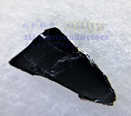
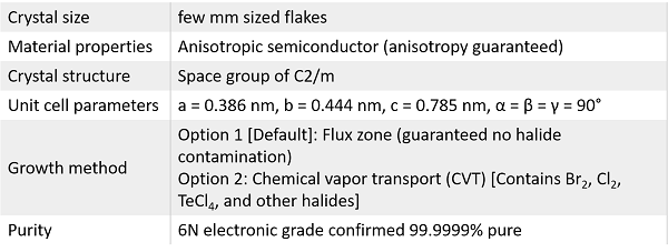
GeP has highly anisotropic dispersions of band structures, with a layer-dependent indirect band gap from (theoretically predicted) 1.68 eV of monolayer to 0.51 eV of bulk. GeP is an anisotropic semiconductor much similar to GaTe monoclinic structure. Our single crystal GeP (Germanium phosphide) crystals come with guaranteed optical, electronic, and structural anisotropy. They are developed at our facilities using state-of-art flux zone techniques. Each growth takes close to three months to provide you perfected crystals that does not contain any halides. Each crystal is highly crystalline, oriented in 0001 direction, and easy to exfoliate. Our R&D staff takes characterization dataset in each sample piece to ensure structural, optical, and electronic consistency.
Characteristics of vdW GeP crystals
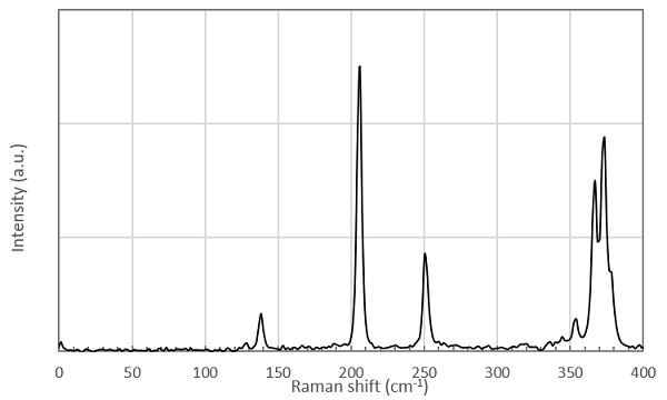
Raman spectrum collected from GeP vdW crystals
XRD Data taken from GeP vdW Crystals

Purity SIMS analysis on GeP crystals

其他服务:
公司客户可以提供晶体免费机械剥离和转移技术。

