库存: 0 件
碳纳米笼
货号:100814 编号:MK1014
CAS号: 规格:
包装:原包装进口 保质期:密封保存6个月+
保存条件:真空密封保存
请选择规格参数
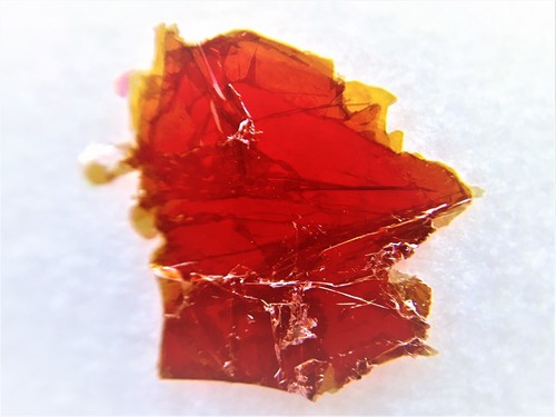
| 样品名称 | 硫化砷锑SbAsS3晶体 |
| 性质 | 半导体 |
| 带隙 | ~1.7 eV |
| 参数 | 尺寸:~ 5-8 mm |
| 应用 | 半导体电子器件,传感器-探测器,非线性光学,STM-AFM实验,光学器件等研究 |
| 其他信息 | 详情请发邮件至:mknano@126.com。 |
硫化砷锑SbAsS3晶体照片:

Our newest class of material: Sb2xAs2(1-x)S3 comes in perfect 1:1:3 stoichiometry consisting of Sb-Sb-S3 atoms. After 34 growth trials in a year, perfect stoichirometry, large single crystal domain size, minimal defect density (1 parts in 100,000 unit cells), and perfected purity level (99.9998%) are achieved. In the bulk form, antimony arsenic sulfide (SbAsS?) is a direct gap semiconductor and has band-gap at around 1.7 eV. Similar to molybdenum disulfide, it has layered structure (lamellar) with weak interlayer coupling and can be isolated down to monolayers. The monolayer thickness measures ~0.8 nm and the monolayer SbAsS? is waiting to be discovered both experimentally and theoretically. Our crystals are large in size ~5-8mm and show remarkable PL characteristics.
Our crystals are grown by state-of-the-art growth techniques over 8 weeks and show high crystallinity. Raman spectrum displays very sharp and clear modes with FWHM less than 6cm-1. Single crystal SbAsS3 comes ready for exfoliation and is ideal for 2D research.
Summary:
Sb2xAs2(1-x)S3 alloys are created by alloying Sb into As2S3.
Please specify your x value when ordering
Space group: P21/c
Layered: Yes / Exfoliates to monolayers
Band gap: ~1.7 eV in bulk
Purity: Semiconductor grade (6N) 99.9999%
Growth technique: Vapor transport technique – Duration: 2.0 months
Sample size: 5-10 mm
其他服务:
公司客户可以提供晶体免费机械剥离和转移技术。

