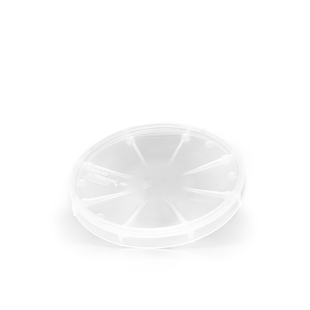
样品照片:

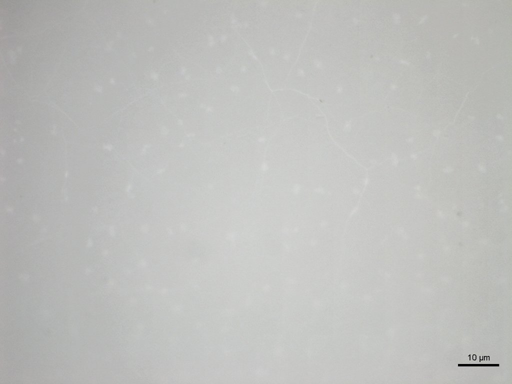
光学显微镜照片:
样品数据:
Monolayer Graphene on PEN- Processed in Clean Room Class 1000
Grown by CVD on copper foil and transferred to polyethylene naphthalate polymer (PEN) using wet transfer process.
GRAPHENE FILM
- · Transparency: > 97%
- · Coverage: > 95%
- · Thickness (theoretical): 0.345 nm
- · FET Electron Mobility on Al2O3: 2000 cm2/Vs
- · Hall Electron Mobility on SiO2/Si: 2000-3500 cm2/Vs
- · Sheet Resistance: 750±50 ?/Sq (1cm x 1cm)
- · Grain size: Up to 10 μm
PEN SUBSTRATE
- · Thickness: 125 μm
- · Roughness: Ra = 1.2 nm; Rms = 1.5 nm
QUALITY CONTROL
All our samples are subjected to a rigorous QC in order to ensure a high quality and reproducibility of the graphene.
- · Raman Spectroscopy: I(G)/I(2D)<0.5; I(D)/I(G)<0.05
- · Optical Microscopy inspection of each individual sample to ensure good transfer quality and purity
If your application requires more specific controls (AFM, SEM...) please do not hesitate to contact us.
APPLICATIONS
Flexible displays, ITO replacement, Graphene research, OLEDs


