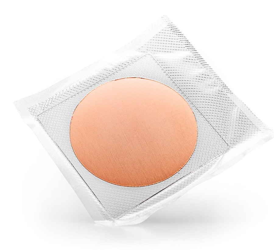
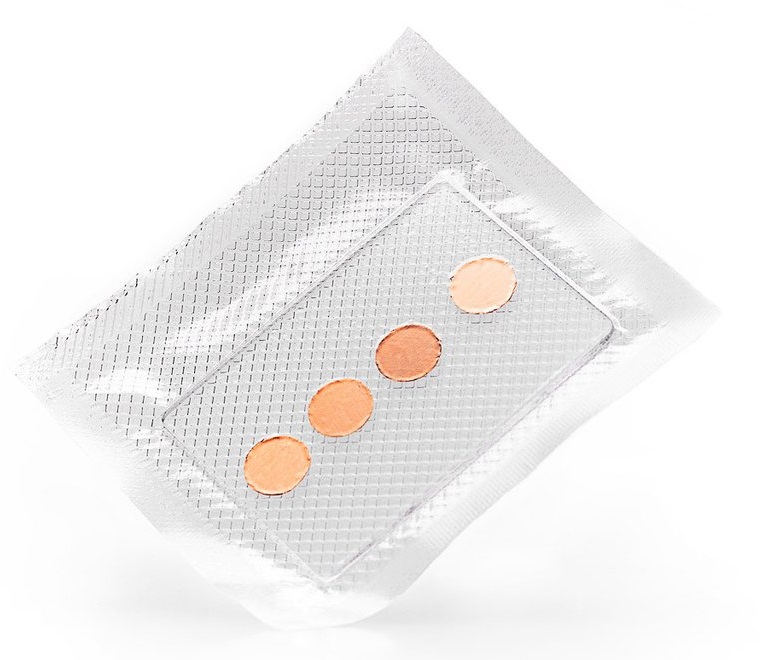
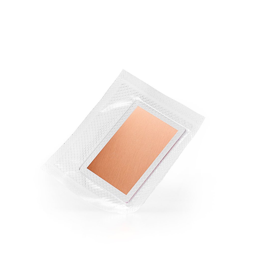
样品照片:
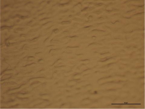
光学显微镜照片:
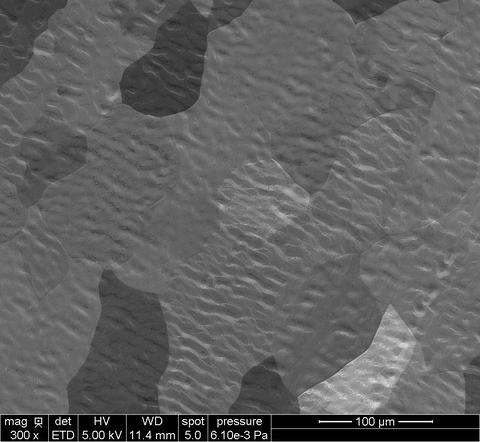
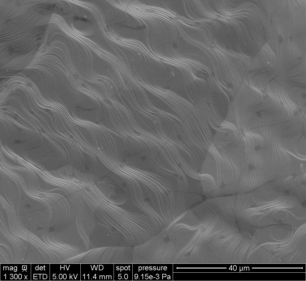
扫描电子显微镜照片:
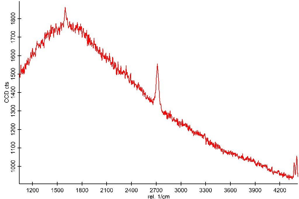
拉曼光谱图:
样品信息:
Monolayer Graphene on Cu with PMMA Coating - Processed in Clean Room Class 1000
A single-layer graphene film on a copper substrate. This product is provided with a PMMA coating on top of the Graphene in order ease the transfer process and to avoid contamination. It's a high quality product, with a great homogeneity, and it is ideal for R&D departments and universities.
GRAPHENE FILM
- · Growth method: CVD synthesis
- · Appearance (color): Transparent
- · Transparency: > 97%
- · Appearance (form): Film
- · Coverage: > 95%
- · Number of graphene layers: 1
- · Thickness (theoretical): 0.345 nm
- · FET Electron Mobility on Al2O3: 2000 cm2/Vs
- · Hall Electron Mobility on SiO2/Si: 2000-3500 cm2/V
- · Sheet Resistance on SiO2/Si: 450±40 Ohms/sq (1cm x1cm)
- · Grain size: Up to 10 μm
SUBSTRATE CU FOIL
- · Thickness: 18 μm
- · Roughness: around 80 nm
- · Pretreated for easier bottom layer removal: Monolayer graphene on the back side of Copper is partially removed, but not completely, so an additional treatment like RIE is needed before transfer to eliminate the bottom layer totally