样品照片:

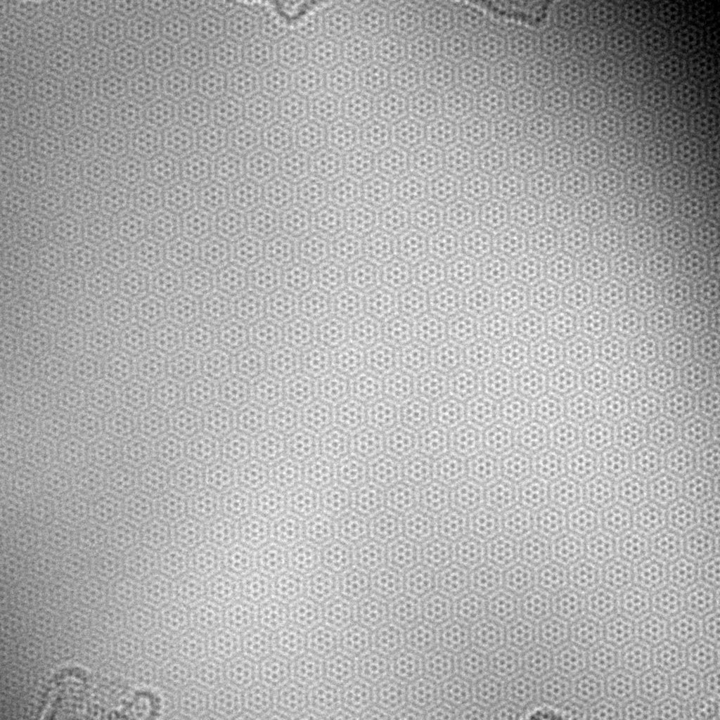
透射电子显微镜照片:
衬底和样品信息:
Bilayer Graphene on SiO?/Si 10 mm x 10 mm (non AB Bernal stacking) - Processed in Clean Room Class 1000
The bilayer graphene product consists of two CVD layers produced by multiple transfer on a SiO2/Si substrate. Lower sheet resistance values can be obtained when compared to monolayer samples.
GRAPHENE FILM
- · Transparency: >94 %
- · Color: Transparent
- · Coverage: >95%
- · Number of graphene layers: 2
- · Thickness (theoretical): 0.69 nm
- · Sheet resistance: 190±30 Ohms/sq (1cm x 1cm)
- · Grain size: Up to 10 μm
SUBSTRATE SIO2/SI
- · Dry Oxide Thickness: 300 nm (+/-5%)
- · Type/Dopant: P/Bor
- · Orientation: <100>
- · Resistivity: <0.005 Ohm·cm
- · Thickness: 525 +/- 20 μm
- · Front surface: Single Side Polished
- · Back Surface: Etched
- · Particles: <10@0.3 μm
APPLICATIONS
Our Graphene Oxide is subjected to a rigorous QC in order to ensure a high quality and reproducibility.
- · Transparent conductors in OLEDs, LEDs, solar cells, etc...
- · Graphene transistors and electronic applications
If your application requires more specific quality control, please do not hesitate to contact us.