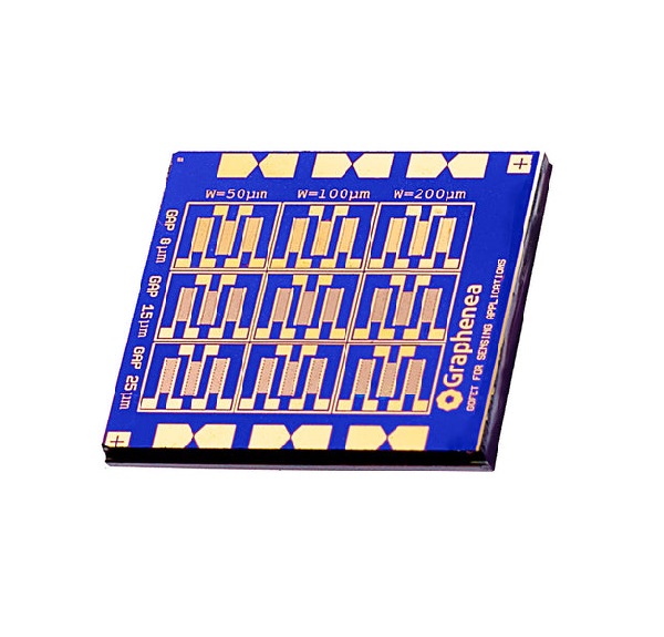
器件照片:


器件光学显微镜数据:


GO表征数据:


DESCRIPTION:
GOFET (Die size 10 mm x 10 mm) - Processed in Clean Room Class 1000. The GOFET chip from Graphenea delivers state-of-the-art graphene oxide devices directly to the researcher to allow application-driven research without the added burden of having to fabricate high-quality devices. The GOFET chip from Graphenea provides 27 graphene oxide (GO) devices distributed in a grid pattern on the chip. All the devices have the same length (≈1mm), but 3 different widths (≈50µm, ≈100µm and ≈200µm). The interdigitated contacts have 3 different gaps (8µm, 15µm and 25µm). The device channels are formed by overlapping of monolayer (>97%) graphene oxide flakes.
TYPICAL SPECIFICATIONS
· Growth method: CVD synthesis
· Chip dimensions: 10 mm x 10 mm
· Chip thickness: 675 μm
· Number of GFETs per chip: 27
· Gate oxide thickness: 90 nm
· Gate oxide material: SiO2
· Resistivity of substrate: 1-10 Ω.cm
· Metallization: Au contacts
· Average channel thickness: ≈ nm
ABSOLUTE MAXIMUM RATINGS
· Maximum gate-source voltage: ± 50 V
· Maximum temperature rating: Above 80 °C GO starts reducing
· Maximum drain-source current density: Above 104A.cm-2 GO starts reducing
QUALITY CONTROL
All our samples are subjected to a rigorous QC in order to ensure a high quality products.
· Optical Microscopy inspection of all the devices
· Raman spectroscopy of each fabrication batch
· Electrical characterisation of each fabrication batch
APPLICATIONS
Graphene Oxide field-effect transistors (GOFETs) have unprecedented sensitivity to the surrounding environment and is an ideal transducer for a variety of sensing applications. Depending on the application, GOFETs can be tuned to be sensitive only to the stimulus of interest and have shown breakthrough performance in areas such as graphene oxide device research, gas sensing, chemical sensing and biosensing.

