
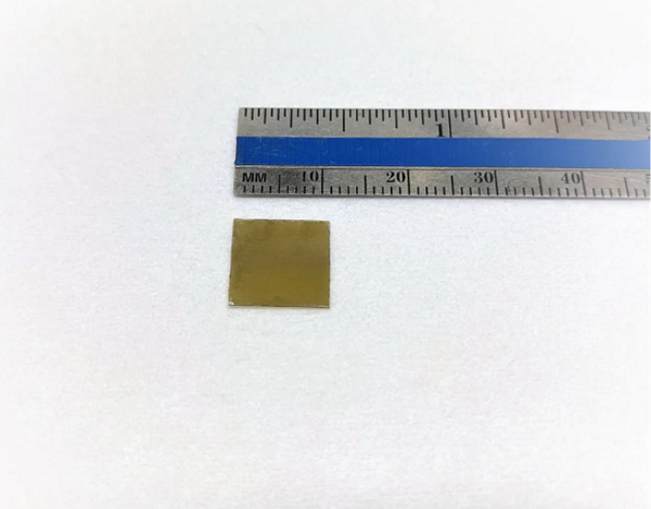
样品照片:

Raman:

This product contains full area coverage WS2 few-layers that measure ~5 layers in thickness. Sheets are grown through chemical vapor deposition technique onto c-cut double side polished sapphire substrates, but layers can be transferred onto other substrates by polymer assisted transfer technique on demand (please select from the drop down menu). The sample measures 1cm2 in size and the entire sample surface contains few-layer thick WS2 sheet. Grown few-layers are high-crystalline as evidenced by HR-TEM, Raman, EDS, and XRD measurements. Please see the datasets in the product images.
Growth method: Our company synthesizes these few layers using chemical vapor deposition (CVD) using highest purity (6N) gases and precursors in semiconductor grade facilities to produce crystalline and large domain size samples (1-50um). Other sources typically use MOCVD or sputtering process wherein defects are very large, domain sizes are small (10nm-500nm), and products are non-layered. Our samples are always highly crystallized, high purity, and perfectly layered.
Sample Properties
| Sample size | 1cm x 1cm square shaped |
| Substrate type | (0001) c-cut sapphire |
| Coverage | Full coverage few-layer thick WS2 |
| Electrical properties | Indirect gap semiconductor |
| Crystal structure | Hexagonal Phase |
| Unit cell parameters | a = b = 0.312 nm, c = 1.230 nm, α = β = 90, γ = 120° |
| Production method | Chemical Vapor Deposition (CVD) |
| Characterization methods | Raman, photoluminescence, TEM, EDS |

