CVD Graphene/CVD Hexagonal Boron Nitride heterostructure on SiO2/Si wafer 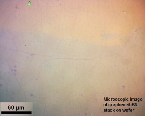 Properties of Graphene/h-BN Film:Single Layer Graphene Film on Single Layer h-BN Film transferred onto 285 nm (p-doped) SiO2/Si wafer Size: 1cmx1cm; 4 pack The thickness and quality of each film is controlled by Raman Spectroscopy The coverage of this product is about 98% The films are continuous, with minor holes and organic residues High Crystalline Quality The graphene film is premodominantly single layer (more than 95%) with occasional small multilayer islands (less than 5% bi-layers) Sheet Resistance: 430-800 Ω/square 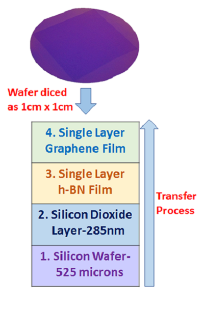
Raman: 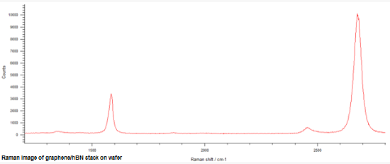
H-BN TEM: 
Properties of Silicon/Silicon Dioxide Wafers:Oxide Thickness: 285 nm; Color: Violet; Wafer thickness: 525 micron Resistivity: 0.001-0.005 ohm-cm;Type/Dopant: P/Boron;Orientation: <100> Front Surface: Polished;Back Surface: Etched Applications: Graphene/hBN interfaces are used where the graphene needs to be precisely gated, for increased mobility, and for reduced scattering. h-BN is appealing as a substrate for graphene-based electronics because its surface is atomically smooth, it is free of dangling bonds, and has an analogous structure to graphene. Using our h-BN on SiO2/Si wafers in conjuction with graphene will encourage you to explore graphene heterostructures for transistor applications Our graphene/h-BN films are manufactured using a PMMA assisted transfer method. Please refer to the references below for more details. We can offer custom sizes of graphene/h-BN films on a 4" wafer. Please contact us at info@graphenelab.com for more details. Academic References / Read MoreGraphene Growth Large-Area Synthesis of High-Quality and Uniform Graphene Films on Copper Foils Science 5 June 2009: Vol. 324. no. 5932, pp. 1312 - 1314 Graphene Transfer Transfer of Large-Area Graphene Films for High-Performance Transparent Conductive Electrodes, Li et.al., Nano Lett., 2009, 9 (12), pp 4359–4363 Toward Clean and Crackless Transfer of Graphene Liang et.al.,ACS Nano, 2011, 5 (11), pp 9144–9153 Graphene/h-BN Heterostructures
Electrical properties and applications of graphene, hexagonal boron nitride (h-BN), and graphene/h-BN heterostructures Materials Today Physics, Science Direct: Vol 2, September 2017, pp 6-34 | 