|
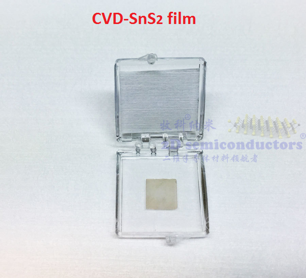
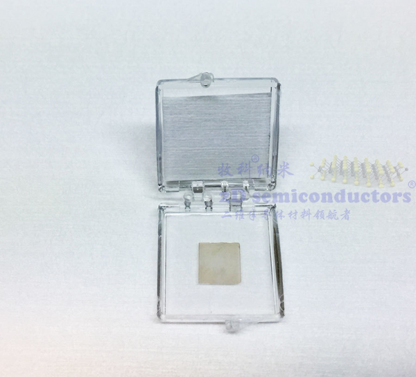
样品照片: 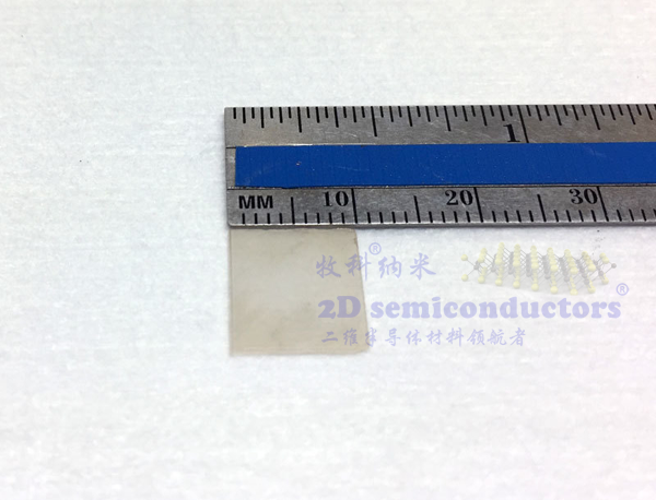
高分辨透射电子显微镜照片: 
EDX: 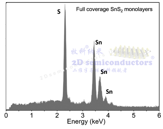
Raman和PL光谱: 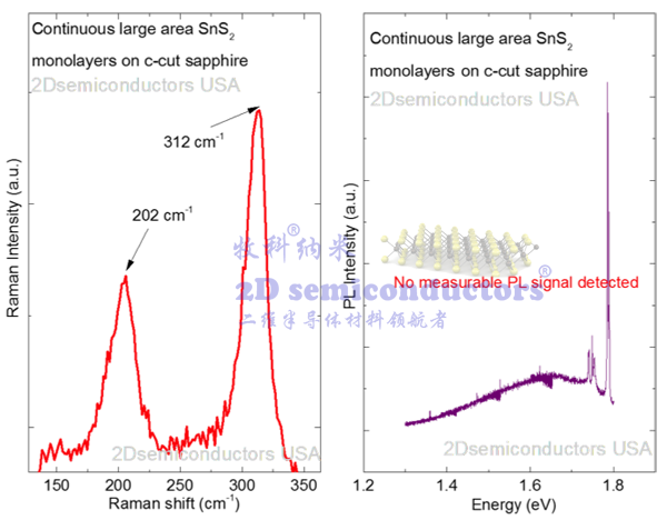
DeScription: This product contains full area coverage SnS2 monolayers on c-cut sapphire substrates. Sample size measures 1cm in size and the entire sample surface contains monolayer thick SnS2 sheet. Synthesized full area coverage monolayer SnS2 is highly crystalline. Growth method: Our company synthesizes these monolayers using chemical vapor deposition (CVD) using highest purity (6N) gases and precursors in semiconductor grade facilities to produce crystalline and large domain size samples (1-50um). This is unlike commonly used MOCVD process wherein defects are very very large and domain sizes are small (10nm-500nm). Sample Properties | Sample size | 1cm x 1cm square shaped | | Substrate type | Sapphire c-cut (0001) | | Coverage | Full monolayer coverage | | Electrical properties | 2.2 eV Indirect Gap Semiconductor | | Crystal structure | Hexagonal Phase | | Unit cell parameters | a = b = 0.362, c = 0.590 nm, α = β = 90°, γ = 120° | | Production method | Low Pressure Chemical Vapor Deposition (LPCVD) | | Characterization methods | Raman, angle resolved Raman spectroscopy, photoluminescence, absorption spectroscopy TEM, EDS |
Specification. - Identification. Full coverage 100% monolayer SnS2 uniformly covered across c-cut sapphire
- Physical dimensions. one centimeter in size. Larger sizes up to 2-inch wafer-scale available upon requests.
- Smoothness. Atomically smooth surface with roughness < 0.15 nm.
- Uniformity. Highly uniform surface morphology. SnS2 monolayers uniformly cover across the sample.
- Purity. 99.9995% purity as determined by nano-SIMS measurements
- Reliability. Repeatable Raman and photoluminescence response
- Crystallinity. High crystalline quality, Raman response, and photoluminescence emission comparable to single crystalline monolayer flakes.
- Substrate. c-cut Sapphire but our research and development team can transfer SnS2 monolayers onto variety of substrates including PET, quartz, and SiO2/Si without significant compromisation of material quality.
- Support. 2Dsemiconductors USA is an American owned, regulated, and operated company. Our customers are well-protected by international as well as strict American customer laws and regulations. We give full technical support and guarantee your satisfaction with our well-established customer
- Defect profile. SnS2 monolayers do not contain intentional dopants or defects. However, our technical staff can produce defected SnS2 using a-bombardment technique.
|