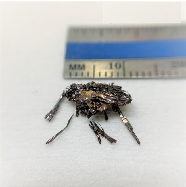
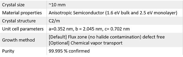
Silicon phosphide (SiP) is a layered semiconductor crystallizing in C2/m (2D anisotropic) structure. It has been shown to undergo indirect (bulk) to direct (monolayer) gap transition from 1.69 (bulk) to 2.5 eV (monolayer). The atoms are arranged to form 1D-like features much similar to black phosphorus, black arsenic, GaTe, and ReS2. Owing to its highly anisotropic atomic arrangement, it has been shown to host anisotropic excitons, thermal conduction, optical absorption, as well as electronic mobility. Our SiP crystals are grown using two different techniques through chemical vapor transport (CVT) or flux zone growth (see description of these two methods below). These crystals are treated as gold standards in 2D materials field owing to perfected optical and electronic behavior. SiP crystals appear to be fibrous (microscale layered ribbons) that are ready for exfoliation as shown in the images.
样品表征:
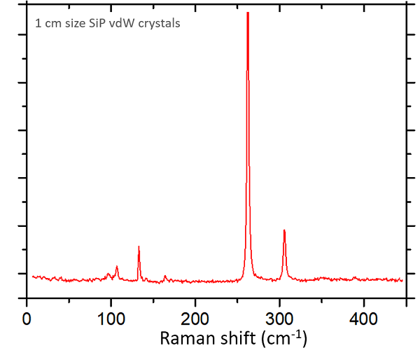
Raman:
其他服务:
公司客户可以提供晶体免费机械剥离和转移技术。