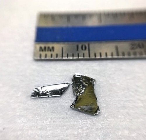
Tin sulfide (SnS) is a layered monochalcogenide semiconductor crystallizing in orthorhombic phase. The layers of cations are separated only by van der Waals (vdW) forces that provide intrinsically chemically inert surface without dangling bonds and surface density of states. Theoretical predictions show that SnS band gap values span from 1.4 eV to 1.9 eV from bulk to monolayer. SnS layers exhibit high in-plane anisotropy and high carrier mobility reaching as high as tens of thousands of cm2V–1s–1 which is superior to that of black phosphorus [1]. Their potential uses include photovoltaics, high electron mobility transistors, and catalytic energy conversion technologies. Our SnS crystal exhibit 99.9999% guaranteed purity, low defect concentration (<1E9cm-2), and high crystallinity. SnS crystals are grown either through flux vapor transport (flux method) or Bridgman technique.
样品表征:
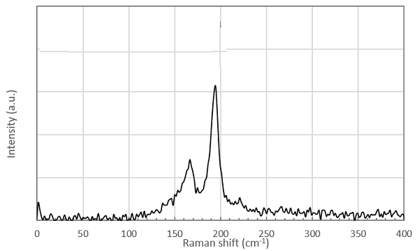
Raman:
EDS:

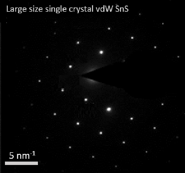
SEAD:
其他服务:
公司客户可以提供晶体免费机械剥离和转移技术。