| 货号 |
编号 |
参数 |
库存 |
价格 |
| 100872 |
MK1072 |
~3-5mm |
100 |
登录查看
|
| 样品名称 | 进口P型二硒化钨单晶 p-type WSe2 | | 性质 | 半导体 | | 带隙 | ~2.0 eV | | 参数 | 尺寸:~3-5mm, | | 应用 | 半导体电子器件,传感器-探测器,光学器件等研究 | | 其他性质 | 详情请发邮件至:mknano@126.com. |
晶体照片: 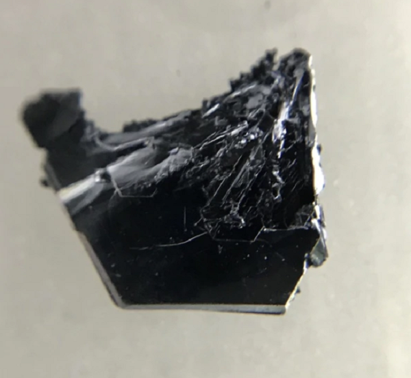
Product Description WSe2 is a semiconductor with an indirect band gap of 1.25 eV in the bulk and 1.62 eV direct optical band gap semiconductor in the monolayer form. Its electronic (single particle) band gap is located at ~2.0 eV with an excitonic binding energy of 0.4 eV. WSe2 layers are stacked together via van der Waals (vdW) interactions which enables them to be exfoliated down to monolayers. p-type WSe2 crystals contain Nb doping (~1E16cm-3 to 1E17 cm-3) to sustain p-type behavior, and are treated as gold standards in 2D materials field. WSe2 crystals from 2Dsemiconductors are known for its superior valleytronic performance, perfect crystallization, defect free structure, extremely narrow PL bandwidths, clean PL spectra (free of bound exciton shoulders), and high carrier mobility. Our WSe2 crystals are grown either flux zone or chemical vapor transport techniques. If your application is solely focusing on optics, photonics, and quantum optics, we strongly recommend flux zone grown WSe2 crystals owing to their perfect crystallinity and extremely low defects concentrations. Thousands of scientific articles have cited us and used these crystals for scientific accuracy and clean signals. Typical characteristics of WSe2 crystals from 2Dsemiconductors 
XRD: 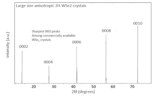
Raman: 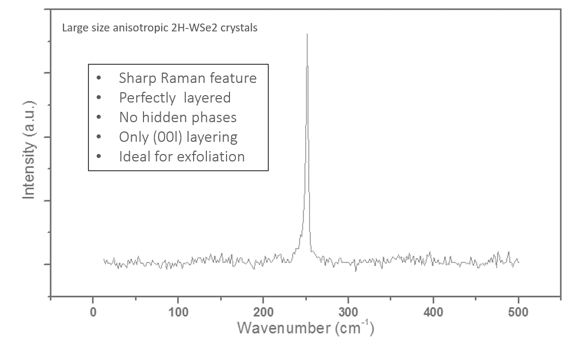
其他服务:
公司客户可以提供晶体免费机械剥离和转移技术。
|