|
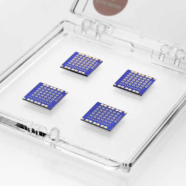
器件图片: 

光学显微镜图: 
器件示意图: 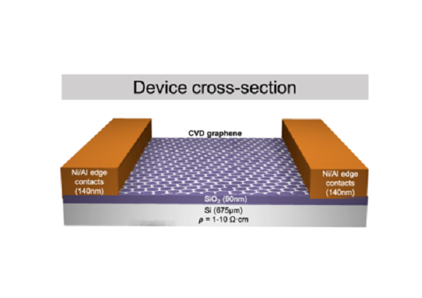
石墨烯拉曼: 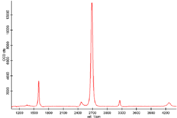
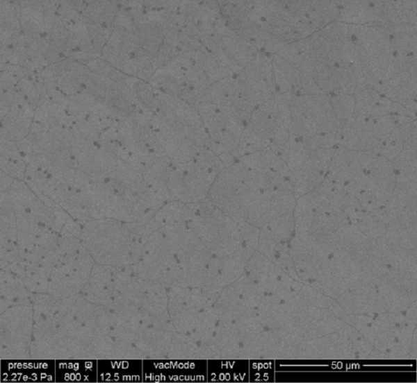
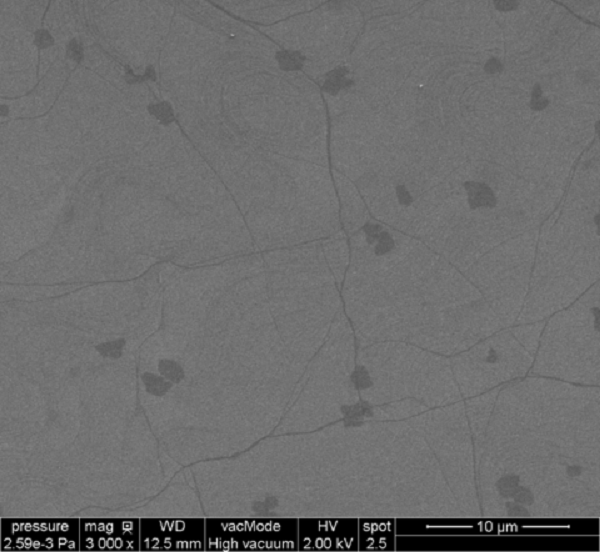
SEM: 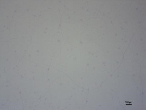
DESCRIPTION: GFET-S10 (Die size 10 mm x 10 mm) - Processed in Clean Room Class 1000 The GFET-S10 chip from Graphenea provides 36 graphene devices distributed in a grid pattern on the chip. Thirty devices have a Hall-bar geometry and six have a 2-probe geometry. The Hall-bar devices can be used for Hall-bar measurements as well as 4-probe and 2-probe devices. There are varying graphene channel dimensions to allow investigation of geometry dependence on device properties. TYPICAL SPECIFICATIONS· Growth method: CVD synthesis · Chip dimensions: 10 mm x 10 mm · Chip thickness: 675 μm · Number of GFETs per chip: 36 · Gate oxide thickness: 90 nm · Gate oxide material: SiO2 · Dielectric Constant of the SiO2 layer: 3.9 · Resistivity of substrate: 1-10 Ω.cm · Metallization: Au contacts · Graphene field-effect mobility: >1000 cm2/V.s · Dirac point: <50 V · Minimum working devices: >75 %
ABSOLUTE MAXIMUM RATINGSQUALITY CONTROL All our samples are subjected to a rigorous QC in order to ensure a high quality products. · Optical microscopy inspection of all the devices · Raman Spectroscopy of each fabrication batch · Electrical characterisation of each fabrication batch APPLICATIONS Graphene field-effect transistors (GFETs) have unprecedented sensitivity to the surrounding environment and is an ideal transducer for a variety of sensing applications. Depending on the application, GFETs can be tuned to be sensitive only to the stimulus of interest and have shown breakthrough performance in areas such as photosensing, magnetic sensing and biosensing.
|