|
样品照片: 
扫描电子显微镜照片: 

拉曼光谱数据: 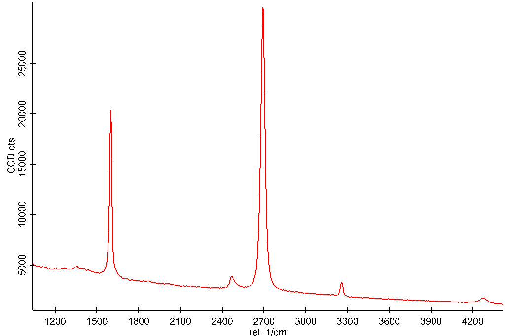
衬底信息和样品信息: Monolayer Graphene film on SiO?/Si (10 mm x 10 mm) - Processed in Clean Room Class 1000 Monolayer Graphene produced by CVD on copper catalyst and transferred to a SiO2/Si substrate using wet transfer process. This product is ideal for R&D departments and universities. GRAPHENE FILM - · Transparency: > 97 %
- · Coverage: > 95%
- · Thickness (theoretical): 0.345 nm
- · FET Electron Mobility on Al2O3: 2000 cm2/Vs
- · Hall Electron Mobility on SiO2/Si: 2000-3500 cm2/Vs
- · Sheet Resistance: 450±40 Ohms/sq (1cm x1cm)
- ·Grain size: Up to 10 μm
SUBSTRATE SIO2/SI - · Dry Oxide Thickness: 300 nm (+/-5%)
- · Type/Dopant: P/Bor
- · Orientation: <100>
- · Resistivity: <0.005 ohm.cm
- · Thickness: 525 +/- 20 μm
- · Front surface: Single Side Polished
- · Back Surface: Etched
- · Particles: <10@0.3 μm
QUALITY CONTROL All our samples are subjected to a rigorous QC in order to ensure a high quality and reproducibility of the graphene. - · Raman Spectroscopy: I(G)/I(2D)<0.7; I(D)/I(G)<0.05
- · Optical Microscopy inspection of each individual sample to ensure good transfer quality and purity
If your application requires more specific quality control (AFM, SEM...) , please do not hesitate to contact us. APPLICATIONS Graphene research, Graphene transistors and electronic applications, Graphene optoelectronics, plasmonics and nanophotonics. Graphene photodetectors (measure photon flux or optical power), Biosensors and bioelectronics, Aerospace industry (electronics, thermal interface materials, etc.), MEMS and NEMS
|