|
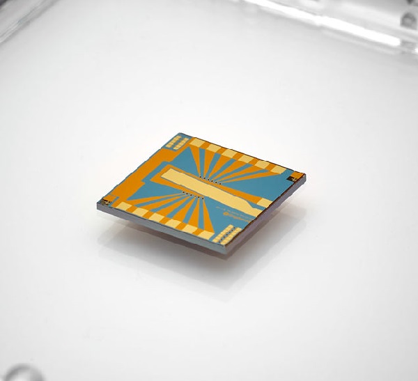
器件照片: 

光学显微镜图: 

器件示意图: 
石墨烯表征数据: 


DESCRIPTION: GFET-S21 (Die size 10 mm x 10 mm) - Processed in Clean Room Class 1000.The GFET S-21 chip from Graphenea is designed for measurements in liquid medium. The new version provides 12 graphene devices connected in parallel, with encapsulation on the metal pads to avoid degradation and reduce leakage currents; the probe pads are located near the periphery of the chip. It also includes a non-encapsulated electrode at the center of the chip, which allows liquid gating without the need of an external gate electrode (such as Ag/AgCl probes). This device architecture enhances signal-to-noise ratio and reduces parasitics. It also removes device-to-device variation, smoothing device response and improving reliability. TYPICAL SPECIFICATIONS · Growth method: CVD synthesis · Chip dimensions: 10 mm x 10 mm · Chip thickness: 675 μm · Number of GFETs per chip: 1 (12 in parallel) · Gate oxide thickness: 90 nm · Gate oxide material: SiO2 · Resistivity of substrate: 1-10 Ω.cm · Metallization: Au contacts · Graphene field-effect mobility: >1000 cm2/V.s · Encapsulation: 50 nm Al2O3 · Dirac point (liquid gating): <1V · Minimum working devices: >75 % ABSOLUTE MAXIMUM RATINGS · Maximum gate-source voltage (liquid gating in PBS): ± 2 V · Maximum temperature rating: 150 °C · Maximum drain-source current density: 107A.cm-2 QUALITY CONTROL All our samples are subjected to a rigorous QC in order to ensure a high quality products. · Optical Microscopy inspection of all the devices · Raman spectroscopy of each fabrication batch · Electrical characterisation of each fabrication batch APPLICATIONS Graphene field-effect transistors (GFETs) have unprecedented sensitivity to the surrounding environment and is an ideal transducer for a variety of sensing applications. Depending on the application, GFETs can be tuned to be sensitive only to the stimulus of interest and have shown breakthrough performance in areas such as graphene device research, chemical sensing, bioelectronics and biosensing.
|