|
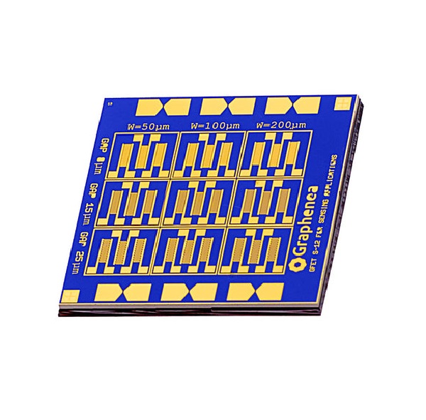
器件照片: 


光学显微镜照片: 


器件示意图: 
石墨烯表征数据: 

DESCRIPTION: GFET-S12 (Die size 10 mm x 10 mm) - Processed in Clean Room Class 1000.The GFET-S12 chip from Graphenea provides 27 graphene devices distributed in a grid pattern on the chip. The devices have interdigitated contacts on top of the graphene channel, which are optimal for sensing of gases and volatile compounds. All the devices have the same channel length (1mm), but 3 different widths (50µm, 100µm and 200µm). The interdigitated contacts have 3 different gaps (8µm, 15µm and 25µm). These different graphene channel dimensions allow investigation of geometry dependence on device properties, enabling immediate device optimization. TYPICAL SPECIFICATIONS · Growth method: CVD synthesis · Chip dimensions: 10 mm x 10 mm · Chip thickness: 675 μm · Number of GFETs per chip: 27 · Gate oxide thickness: 90 nm · Gate oxide material: SiO2 · Dielectric Constant of the SiO2 layer: 3.9 · Resistivity of substrate: 1-10 Ω.cm · Metallization: Au contacts · Graphene field-effect mobility: >1000 cm2/V.s · Dirac point: <50 V · Minimum working devices: >75 %
ABSOLUTE MAXIMUM RATINGS · Maximum gate-source voltage: ± 50 V · Maximum temperature rating: 150 °C · Maximum drain-source current density 107A.cm-2
QUALITY CONTROL All our samples are subjected to a rigorous QC in order to ensure a high quality products. · Optical microscopy inspection of all the devices · Raman Spectroscopy of each fabrication batch · Electrical characterisation of each fabrication batch APPLICATIONS Graphene field-effect transistors (GFETs) have unprecedented sensitivity to the surrounding environment and is an ideal transducer for a variety of sensing applications. Depending on the application, GFETs can be tuned to be sensitive only to the stimulus of interest and have shown breakthrough performance in areas such as graphene device research, quantum transport, gas sensors and chemical sensors.
|