|
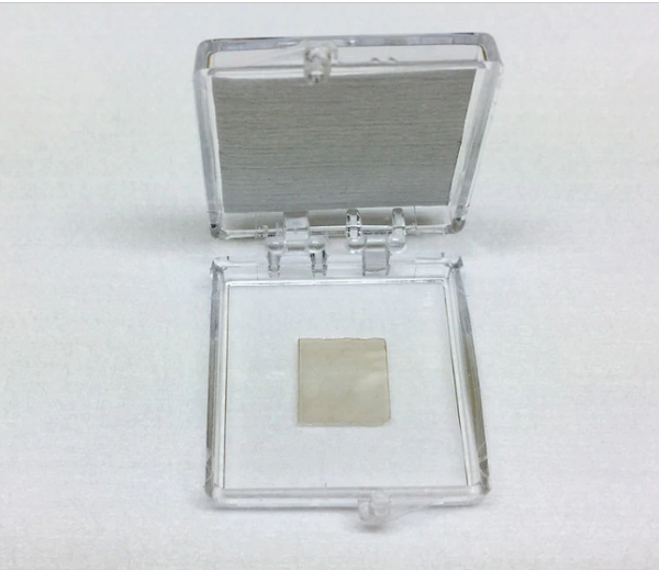
样品照片: 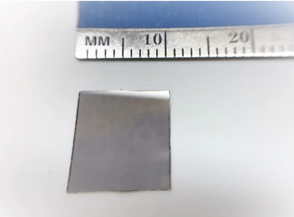
样品信息: 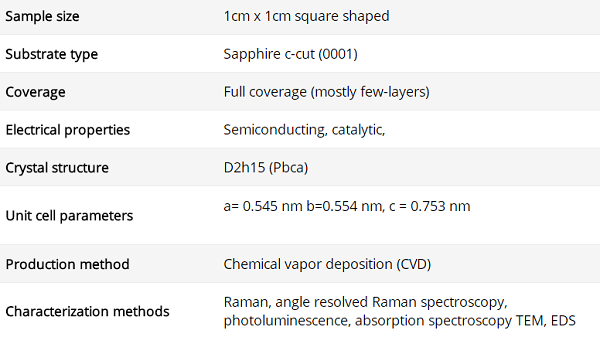
Description PdS2 is vdW material with excellent catalytic and semiconducting properties. Full area coverage PdS2 layers on c-cut sapphire substrates has been grown using modified chemical vapor deposition technique. Sample size measures 1cm in size and the entire sample surface contains PdS2 sheets. Growth method: Our company synthesizes these monolayers using chemical vapor deposition (CVD) using highest purity (6N) gases and precursors in semiconductor grade facilities to produce crystalline and large domain size samples (1-50um). This is unlike commonly used MOCVD process wherein defects are very very large and domain sizes are small (10nm-500nm).
|